- 您现在的位置:买卖IC网 > Sheet目录3886 > PIC16C54C-04/SO (Microchip Technology)IC MCU OTP 512X12 18SOIC
PIC18F2450/4450
2006 Microchip Technology Inc.
Advance Information
DS39760A-page 63
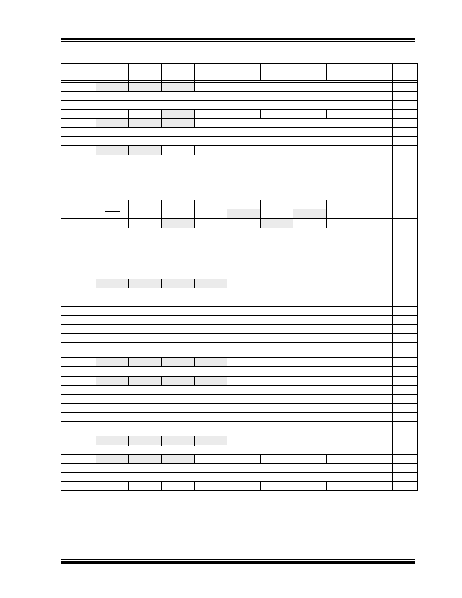
TABLE 5-2:
REGISTER FILE SUMMARY (PIC18F2450/4450)
File Name
Bit 7
Bit 6
Bit 5
Bit 4
Bit 3
Bit 2
Bit 1
Bit 0
Value on
POR, BOR
Details
on page
TOSU
—
Top-of-Stack Upper Byte (TOS<20:16>)
---0 0000
TOSH
Top-of-Stack High Byte (TOS<15:8>)
0000 0000
TOSL
Top-of-Stack Low Byte (TOS<7:0>)
0000 0000
STKPTR
STKFUL
STKUNF
—
SP4
SP3
SP2
SP1
SP0
00-0 0000
PCLATU
—
Holding Register for PC<20:16>
---0 0000
PCLATH
Holding Register for PC<15:8>
0000 0000
PCL
PC Low Byte (PC<7:0>)
0000 0000
TBLPTRU
—
—bit 21(1)
Program Memory Table Pointer Upper Byte (TBLPTR<20:16>)
--00 0000
TBLPTRH
Program Memory Table Pointer High Byte (TBLPTR<15:8>)
0000 0000
TBLPTRL
Program Memory Table Pointer Low Byte (TBLPTR<7:0>)
0000 0000
TABLAT
Program Memory Table Latch
0000 0000
PRODH
Product Register High Byte
xxxx xxxx
PRODL
Product Register Low Byte
xxxx xxxx
INTCON
GIE/GIEH
PEIE/GIEL
TMR0IE
INT0IE
RBIE
TMR0IF
INT0IF
RBIF
0000 000x
INTCON2
RBPU
INTEDG0
INTEDG1
INTEDG2
—TMR0IP
—RBIP
1111 -1-1
INTCON3
INT2IP
INT1IP
—
INT2IE
INT1IE
—INT2IF
INT1IF
11-0 0-00
INDF0
Uses contents of FSR0 to address data memory – value of FSR0 not changed (not a physical register)
N/A
POSTINC0
Uses contents of FSR0 to address data memory – value of FSR0 post-incremented (not a physical register)
N/A
POSTDEC0
Uses contents of FSR0 to address data memory – value of FSR0 post-decremented (not a physical register)
N/A
PREINC0
Uses contents of FSR0 to address data memory – value of FSR0 pre-incremented (not a physical register)
N/A
PLUSW0
Uses contents of FSR0 to address data memory – value of FSR0 pre-incremented (not a physical register) –
value of FSR0 offset by W
N/A
FSR0H
—
Indirect Data Memory Address Pointer 0 High Byte
---- 0000
FSR0L
Indirect Data Memory Address Pointer 0 Low Byte
xxxx xxxx
WREG
Working Register
xxxx xxxx
INDF1
Uses contents of FSR1 to address data memory – value of FSR1 not changed (not a physical register)
N/A
POSTINC1
Uses contents of FSR1 to address data memory – value of FSR1 post-incremented (not a physical register)
N/A
POSTDEC1
Uses contents of FSR1 to address data memory – value of FSR1 post-decremented (not a physical register)
N/A
PREINC1
Uses contents of FSR1 to address data memory – value of FSR1 pre-incremented (not a physical register)
N/A
PLUSW1
Uses contents of FSR1 to address data memory – value of FSR1 pre-incremented (not a physical register) –
value of FSR1 offset by W
N/A
FSR1H
—
Indirect Data Memory Address Pointer 1 High Byte
---- 0000
FSR1L
Indirect Data Memory Address Pointer 1 Low Byte
xxxx xxxx
BSR
—
Bank Select Register
---- 0000
INDF2
Uses contents of FSR2 to address data memory – value of FSR2 not changed (not a physical register)
N/A
POSTINC2
Uses contents of FSR2 to address data memory – value of FSR2 post-incremented (not a physical register)
N/A
POSTDEC2
Uses contents of FSR2 to address data memory – value of FSR2 post-decremented (not a physical register)
N/A
PREINC2
Uses contents of FSR2 to address data memory – value of FSR2 pre-incremented (not a physical register)
N/A
PLUSW2
Uses contents of FSR2 to address data memory – value of FSR2 pre-incremented (not a physical register) –
value of FSR2 offset by W
N/A
FSR2H
—
Indirect Data Memory Address Pointer 2 High Byte
---- 0000
FSR2L
Indirect Data Memory Address Pointer 2 Low Byte
xxxx xxxx
STATUS
—
—N
OV
Z
DC
C
---x xxxx
TMR0H
Timer0 Register High Byte
0000 0000
TMR0L
Timer0 Register Low Byte
xxxx xxxx
T0CON
TMR0ON
T08BIT
T0CS
T0SE
PSA
T0PS2
T0PS1
T0PS0
1111 1111
Legend:
x
= unknown, u = unchanged, - = unimplemented, q = value depends on condition. Shaded cells are unimplemented, read as ‘0’.
Note
1:
Bit 21 of the TBLPTRU allows access to the device Configuration bits.
2:
The SBOREN bit is only available when BOREN<1:0> = 01; otherwise, the bit reads as ‘0’.
3:
These registers and/or bits are not implemented on 28-pin devices and are read as ‘0’. Reset values are shown for 40/44-pin devices;
individual unimplemented bits should be interpreted as ‘-’.
4:
RA6 is configured as a port pin based on various primary oscillator modes. When the port pin is disabled, all of the associated bits read ‘0’.
5:
RE3 is only available as a port pin when the MCLRE Configuration bit is clear; otherwise, the bit reads as ‘0’.
6:
RC5 and RC4 are only available as port pins when the USB module is disabled (UCON<3> = 0).
发布紧急采购,3分钟左右您将得到回复。
相关PDF资料
PIC16F722-I/ML
IC PIC MCU FLASH 2KX14 28-QFN
PIC16LCE623T-04I/SO
IC MCU CMOS.5K OTP W/EEPRM18SOIC
PIC16HV540-04I/SO
IC MCU OTP 512X12 18SOIC
PIC16LCE623T-04E/SS
IC MCU CMOS.5K OTP W/EEPRM20SSOP
PIC16LCE623T-04E/SO
IC MCU CMOS.5K OTP W/EEPRM18SOIC
5-520415-4
CONN TRIOMATE 4POS VERT TIN
6-176982-6
CONN TRIO-MATE 16POS .100 FFC
PIC16LCE623-04I/SO
IC MCU CMOS.5K OTP W/EEPRM18SOIC
相关代理商/技术参数
PIC16C54C-04/SO
制造商:Microchip Technology Inc 功能描述:8BIT CMOS MCU SMD 16C54 SOIC18
PIC16C54C-04/SO
制造商:Microchip Technology Inc 功能描述:Microcontroller IC Number of I/Os:12
PIC16C54C-04/SS
功能描述:8位微控制器 -MCU .75KB 25 RAM 12 I/O 4MHz SSOP20 RoHS:否 制造商:Silicon Labs 核心:8051 处理器系列:C8051F39x 数据总线宽度:8 bit 最大时钟频率:50 MHz 程序存储器大小:16 KB 数据 RAM 大小:1 KB 片上 ADC:Yes 工作电源电压:1.8 V to 3.6 V 工作温度范围:- 40 C to + 105 C 封装 / 箱体:QFN-20 安装风格:SMD/SMT
PIC16C54C-04E/P
功能描述:8位微控制器 -MCU .75KB 25 RAM 12 I/O 4MHz ExtTemp PDIP18 RoHS:否 制造商:Silicon Labs 核心:8051 处理器系列:C8051F39x 数据总线宽度:8 bit 最大时钟频率:50 MHz 程序存储器大小:16 KB 数据 RAM 大小:1 KB 片上 ADC:Yes 工作电源电压:1.8 V to 3.6 V 工作温度范围:- 40 C to + 105 C 封装 / 箱体:QFN-20 安装风格:SMD/SMT
PIC16C54C-04E/SO
功能描述:8位微控制器 -MCU .75KB 25 RAM 12 I/O 4MHz Ext Temp SOIC18 RoHS:否 制造商:Silicon Labs 核心:8051 处理器系列:C8051F39x 数据总线宽度:8 bit 最大时钟频率:50 MHz 程序存储器大小:16 KB 数据 RAM 大小:1 KB 片上 ADC:Yes 工作电源电压:1.8 V to 3.6 V 工作温度范围:- 40 C to + 105 C 封装 / 箱体:QFN-20 安装风格:SMD/SMT
PIC16C54C-04E/SS
功能描述:8位微控制器 -MCU .75KB 25 RAM 12 I/O 4MHz Ext Temp SSOP20 RoHS:否 制造商:Silicon Labs 核心:8051 处理器系列:C8051F39x 数据总线宽度:8 bit 最大时钟频率:50 MHz 程序存储器大小:16 KB 数据 RAM 大小:1 KB 片上 ADC:Yes 工作电源电压:1.8 V to 3.6 V 工作温度范围:- 40 C to + 105 C 封装 / 箱体:QFN-20 安装风格:SMD/SMT
PIC16C54C-04I/P
功能描述:8位微控制器 -MCU .75KB 25 RAM 12 I/O 4MHz IndTemp PDIP18 RoHS:否 制造商:Silicon Labs 核心:8051 处理器系列:C8051F39x 数据总线宽度:8 bit 最大时钟频率:50 MHz 程序存储器大小:16 KB 数据 RAM 大小:1 KB 片上 ADC:Yes 工作电源电压:1.8 V to 3.6 V 工作温度范围:- 40 C to + 105 C 封装 / 箱体:QFN-20 安装风格:SMD/SMT
PIC16C54C-04I/P
制造商:Microchip Technology Inc 功能描述:IC 8BIT CMOS MCU 16C54 DIP18